Thursday, July 29, 2010

Experiment 5 complete


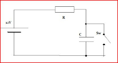
For this experiment i had to build a circuit with 2 different capacitors rated at 100 uF and 330 uF, and 3 different resistors at 100 ohms, 470 ohms and 1K. Then I calculated the time the capacitor would reach full charge by using the formula T (Time) = R (Resistance) x C (Capacitance) x 5 (Number of Steps).


My first test was with the 100uF capacitor and 1K resistor. I calculated the amount of time for the capacitor to fully charge by using the formula T=RxCx5. (1 x 100 x 5) = 500ms to fully charge. Then using the oscilloscope I measured the actual time it took the capacitor to fully charge using the 200ms per division setting.


My next test was using the same 100 uF capacitor, but replacing the 1K for a 100R. 0.1 x 100 x 50ms to fully charge. Using the oscilloscope at the slowest pace possible (200ms per diversion,) I could only estimate the amount of time it took, because the capacitor fully charged before I had time to measure anything, so I just recorded my calculation of 50ms.


Next was the 100uF and 470R. 0.47 x 100 x 5 = 235ms. Measuring with the oscilloscope I recorded 200ms.


Now using a bigger capacitor (330uF) and replacing the 470R with a 1K I calculated the time this capacitor would fully charge. 1 x 330 x 5 = 1650ms. Then using the oscilloscope I meausered a time of 1800ms to fully charge.


Changes with the resistor size will effect the charging time by restricting more current or not restricting as much current. The bigger the resistor, the longer time it will take for the capacitor to charge because of the increased resistance. The smaller the resistor, the less time it will take to charge the capacitor from the decreased resistance.

Changes in the capacitor size will effect the charging time. If a bigger capacitor is used, the longer the time it will take to fully charge would increase. A smaller capacitor will take less time to fully charge.

Wednesday, July 28, 2010

Self Test #1 Complete


Sketch the symbals and label the leads for the two and three terminal devices

NPN.


MOSFET.
LED

ZENER DIODE
Q2. Fill in the blanks


Q3.

Q4: If V=IR and P=IV, what is P in terms of V and R
P=V2R

Vd = 0.7V. Diodes only require 0.7V to operate.


Q6, Vs=50V R1= 10Ohms Diode = 1W Max


Current Flow = (50-0.7)/10= 4.93 Amps


Q7, Pd=IdxVd Id=4.93, Vd=0.7 4.93 x 0.7 = 3.45W


Q8, Yes the diode will be destroyed. The maximum watt dissipation for the Diode is 1 watt and the total amount of watts this circuit will create on the diode will be too great for the diode to control.


Q9, Sketch a simple voltage regulator using discreet components


The zener diode acts as a 5V regulator, so any component placed on the same track as the zener diode will recieve 5V from the Zener Diode opposed from the 12v power supply.


Q10, Is the zener diode in the foward or reverse bias arrangement. Reverse

Experiment 7 complete


With experiment 7 I was asked to construct a circuit with a 15V power supply, a 1K Ohms resistor at Rc and a 10K Ohms resistor at Rb and a BC547 NPN type transistor.


This is a Common Emitter, or open collector circuit because the Emittor has a common connection to both the input and output.

With the circuit connected to a power supply, I connected my voltmeter across the Base and Emitter and recorded .801V. This is because the Vbe only requires 0.7 volts to operate.

I then connected my multimeter across the collector and emitter and recorded 53.7mV. This is because the transistor is saturated and fully open, letting current flow through Vce.


In the saturated state, the transistor is fully on, meaning the switch is closed and the collector and emitter junctions are in forward bias.The Cut Off region is when the transistor is fully off, or the switch is open meaning the transistor is fully off. From this graph I can see that If the Vce was at 3V, The power dissipated by using Pd=Vce x Ic. If the Vce is 3v, then the current at Ic is 14mA. Then Pd will be 3 x 14 = 42mW

Using the graph I can also get the current gain (Beta) of this transistor. If the Vce was 2 volts, Ib = 0.8mA and Ic = 20mA. Beta = Ic/Ib, so 20/0.8 25Beta 3v=14/0.5=28Beta 4v = 5/0.2 = 25 Beta


Thursday, July 22, 2010

Experiment 6 complete

After obtaining 2 different transistors, one a BC547 and the other a TIP32C, I was asked to identify the legs on each transistor and state whether it was a PNP or NPN type. Because i've already explained how to identify a NPN or PNP type and identify which legs the base, collector and emitter were I could do it in a minimum amount of time.

With my multimeter I tested the BC547 transistor and found out that it was a NPN type, and then tested TIP32C and found out it was a PNP Type. Now that i knew which type both transistors were i could then measure the voltage drop across their 3 pins and record the data on this sheet.


Here is a photo of me measuring the Vbc by using the Diode test function on my TIP32C PNP type transistor. My negative lead is on the left leg, which is the base on this PNP type transistor, and my positive lead is on the middle leg which is the collector pin.


Note that my positive lead is on the mounting tab of the transistor. This is because the top terminal is also connected to middle pin, or leg.

Experiment 3 complete

For experiment 3 I used a Vs of 12V, 2 resistors both rated at 100 Ohms and a 5V1 zener diode connected in reverse bias.


My first task was to measure the voltage across the Zener Diode, and recorded 4.95V.
Then I was to vary the voltage to 10V and 15V and recorded 4.70V and 5.06V.

As the Vs of 12V passes through the 1st resistor it reaches the Zener Diode. The zener Diode rated at 5V1 then starts operating and lets current through. The 1st resistor acts as a current limiting resistor and has a Pd of 7V from being connected in series with the Zener Diode. The 2nd resistor is the load.

Because the zener diode has a breakdown region of 5v1 it acts as a 5V1 Regulator circuit.

Reversing the polarity of the Zener diode into forward bias gave me a reading of 0.852V. This is because when the zener diode is connected in forward bias, it acts the same as a normal diode.

Wednesday, July 21, 2010

Experiment 8

Testing a BC547 in it's Saturated switch and active amplifying region.


For this experiment I set up a circuit with a 470R at Rc, an LED and BC547 NPN transistor, and alternated 5 different value resistors 47K, 220K, 270K, 330K and 1M, to be used at Rb.


For this experiment I measured voltage drop and current through the transistor pins as I put different resistors in place and record them on a chart.


I can see from this chart that Vce changed dramatically as more resistance was added. This is because as more resistance was added, the transistor switched from being fully open (Saturated) to Amplifying (Active).


As I increased resistance from 47k to 1M the voltage across Vbe stayed the same. This is because Vbe only requires 0.7 volts to operate. Increasing the resistance will only decrease the current to Ib, it will not decrease the voltage.

Ib decreased from the increased resistance because as Ohms Law illustrates, V=IR. So if more resistance is added to a set voltage, the current will decrease.

Ic decreased from the added resistance, but not as much as Ib because only a 470R was used for Ic, whilst Ib had a much larger resistance rating varying from 47K-1M


This graph is used to calculate the DC current gain of the transistor. Ib is the current at the Base of the transistor and Ic is the current at the Collector. If the Vce was 3 volts, I could use the load line to find the gain or (Beta). We can see that Ib will be 0.5 mA and Ic will be 14mA. To calculate Beta I can use the formula Beta=Ic/Ib. 14/0.5=28.

The Active region is when the transistor is neither fully open or fully closed. The transistor is amplifying small signals

On this graph I can see two new regions. The Saturated region is best described when connected as a switching circuit. It is when the switch is fully open, and allowing current to flow through.

The Cut Off region is when there is not enough power at Vbe to allow current to go though, meaning the switch is closed and no current will flow through.


Experiment 2 complete

For experiment 2 I obtained a 1N4007 Si Diode and an LED. I identified the Anode and Cathode and measured both the LED and Diode in forward bias. The diode gave me a reading of .540V whilst the LED gave me a OL sign. I then measured both components in reverse bias and both components gave me a readout of OL.
I was able to identify the Anode and Cathode by a silver band printed onto the Cathode side of the Diode. The LED had a flat spot on the LED and the positive leg is longer.

I then obtained the data sheet for my 1N4007 Si Diode.

This chart has all the specifications of the 1N4007 diode that i will use in the following circuit.
From this chart i can see that the diode dissipates 2.5W at 25 degrees Celsius. But if i wanted to work out if the diode will be destroyed say for example in a hot day in Brisbane recorded at 42' Celsius, i would then need to do derate the device by 20mW for every degree above 25 as stated in the data sheet.

42 - 25 = 17. This is the number which will be derated. 17 x 20mW = 340mW or 0.340W, So the power dissipation at 42'C equals 2.5 - 0.3 = 2.2 mW. As 2.2 mW is less then the maximum amount of voltage being dissipated by the diode, the diode will not be destroyed.


With this knowledge of my 1N4007 diode i then constructed a circuit with a Vs 5v, 1K as R, and 1N4007 as D.

Using Ohms Law i calculated the amount of amps that will be flowing through the diode. 5V/1000 Ohms = 0.005A or 5mA. Then using my Ampmeter, I calculated the actual amount of amps flowing through the diode and recorded 4.7mA. This reading was as I expected as i had calculated the Diode would have a current of 5mA through it.

Then I was to measure the voltage drop across the Diode, but first I used my measurement which I calculated by subtracting Vd from the resistor which would be around 4.3V from the 5V power supply. Leaving a 0.7 Vd across the diode. When I measured the actual VD when connected to the circuit, I recorded .645V.

Using the data sheet above i obtained the maximum amount of current that could flow through the diode by looking at the Rectified current @ 75'C which is 1 Amp.

Now I calculated the maximum amount of Voltage that could flow through the diode before being destroyed by using the Power Law. Pd=VdxId. We already know that the maximum amount of Pd cant exceed 2.5W as listed in the datasheet, And that the resistor is 1K.

If we use 350V-0.7/1000 Ohms it equals 3.493A. 3.493 x 0.7 =2.44W. 350V is the maximum amount of voltage this diode can handle using a 1K resistor.

Replacing the Diode with an LED i calculated the current by using Ohms law 5V/1000 Ohms = 0.005 Amps or 5mA. I then measured the current flowing through the circuit and recorded 3.05mA.

From this I observed that when I replaced the diode with the LED, the current dropped. If the voltage was the same when I replaced the components and the current decreased, then the resistance has been increased. Therefore the LED has more resistance then the 1N4007 Diode.


Experiment 1 complete


For experiment 1 I obtained 6 resistors of different values. I can tell they are of different value by the different colour bands on them. I then calculated the value of each resistor by using my colour code. The 1st resistor was brown, black, red, then gold. I then converted that information into a number which came out as 1,000 Ohms with 5% tolerance. (950 to 1050 Ohms) I then proceeded with the other 5 resistors and got values of
Brown, Black, Brown, Gold = 100 ohms with 5% tolerance (95-105 Ohms) Yellow, Violet, Brown, Gold = 470 Ohms with 5% tolerance(446.5-47.35 Ohms).
Brown, Black Orange, Gold = 10k with 5% tolerance (9500k-10500k).
Yellow, Violet, Orange, Gold = 47k with 5% tolerance (44.65k-47.35k)
Red, Red, Yellow, Gold = 220k with 5% tolerance. (209k-231k)
I then used my ohmeter and measured the value of each resistor and recorded its value.
My 100 Ohms resistor was 98.1 Ohms, 470 was 458 Ohms, 10k was 9.87k, 47k was 46.7k, 220k was exactly 220k.

I then took the two lowest value resistors and calculated the total resistance in series.
R1 + R2 = Rt 458 + 98.1 = 556.1 Ohms.
I then measured the total resistance with my Ohmeter and recorded 555 Ohms

Then I calculated the total resistance in parallel
Rt = R1 x R2/ R1 + R2 458 x 98.1 = 44929 458 + 98.1 = 556 44929/556 = 80.80 Ohms
I then measured the total resistance with my Ohmeter and recorded a total of 80.54 Ohms.

Alternatively, a formula of 1/458+1/98.1=0.012377086 1/0.012377086= 80.80 Ohms
With this information I have demonstrated, I can explain the principles of resistors paired in series and parallel.

Resistors in series are added together to get the resistance total whilst resistors in parallel are always less then any of the individual resistances. An easy way to calculate Rt with 2 equal resistors is to just half the amount of one resistor. For example two 100 ohm resistors connected in parallel will give a resistance total of 50 Ohms.

Transistors

BJT or Bipolar Junction Transistors are either PNP or NPN semiconductors.

Identifying Transistors

They are easy to identify by using the Diode Tester on my multimeter. I will need to find the base, emitter and collector.

In order to first find the base i take my positive probe and place it on a pin. I then alternate my black probe between the 2 remaining legs. If i don't get a positive reading i know that my positive probe is on the wrong leg. I then alternate legs until eventually i get a positive reading on both legs when i alternate the black probe. If i still dont get a reading i will then switch my positive probe for my negative probe and alternate my positive probe on the pins. Once i find the base, i can identify what type of transistor it is. Either PNP or NPN. To find this out (for example) if my positive probe is on the base and i get a reading when i alternate my negative probe on both legs I have a NPN transistor. This is because i have 2 negatives and 1 positive leg. If my negative probe is on the base and i alternate my positive probe on the other 2 legs and get a reading, i have a PNP transistor. Now that i have identified what kind of transistor i have, i can then work out which pin is the Emitter, and which is the collector. If i am using a NPN type transistor and i have a reading of 0.763V on one pin and 0.767V on the other, the pin with 0.767 is the emitter. This is because the emitter has a higher reading then the collector.
This is due to the disparity in doping concentration between the emitter and collector regions of the transistor. The emittor is a much more heavily doped piece of semiconductor then the collector, causing its juction with the base to produce a higher voltage voltage drop (ref http://www.allaboutcircuits.com/vol_3/chpt_4/3html)
.

Experiment 4 complete

In this experiment I used a 1k ohms resistor, 5v1 Zener diode connected in reverse bias and a 1N4007 Si Diode connected in forward bias with the circuit set up in series. I can immediatly predict V1 from previous experiments with zener diodes in reverse bias by understanding that the Zener diode connected in reverse bias has a breakdown voltage of 5.1V, therefore V1 will be 5.1V. I can also predict V2 by knowing that the silicone diode has a knee voltage of 0.7 Volts, and will operate once this 0.7 volts has been reached. The diode does not require any excess amount of voltage so V2 will be 0.7V. With this knowledge i can get V3 by adding these voltages together. V3 = 5.1V + 0.7V = 5.8V. Because this circuit is in series i can now get V4 by subtracting V3 from Vs. V4 = 10V - 5.8V = 4.2V.

Then measuring the voltage drop with my voltmeter i recorded the results using 10V and 15V.

In my recordings I noticed that the voltage drop across the diodes did not change when i varried the Voltage from 10V to 15V. This is because the zener diode constantly regulates the voltage to 5V1, and the 1N4007 diode only requires 0.7V to operate. The resistor on the other hand almost doubled the amount of voltage drop on itself when I increased the Vs to 15v. This is because the sum of V3 will always equate to 5.8V.

Tuesday, July 20, 2010

Diode Information

Diodes
Diodes are components to prevent current from flowing both ways
In forward bias, the Diode will only operate on as much voltage as the knee voltage.
Silicon diodes have a knee voltage of 0.7 volts

The knee voltage is the amount of voltage needed for the diode to let electrons through.
The breakdown region is when there is too much reverse voltage for the diode to prevent electrons flowing in reverse bias and cannot operate.


Zener Diodes
Zener Diodes also have a knee voltage of 0.7 volts.
Zener diodes have a preset breakdown voltage which will let electrons flow when the correct amount of voltage is applied in reverse bias.

Resistor Colour Codes


1st and 2nd Band

Black = 0
Brown = 1
Red = 2
Orange = 3
Yellow = 4
Green = 5
Blue = 6
Violet = 7
Grey = 8
White = 9

3rd Band

Multiply by number of zero's

4th band

Tolerance

Brown 1%
Red 2%
Gold 5%
Silver 10%
Green 0.5%
Blue 0.25%
Violet 0.1%
If the resistor has 5 bands, the first 3 bands you convert on the colour chart and get 3 numbers. The 4th band will be the multiplier and the 5th will be the tolerance of the resistor.